 Microcontrollers & architecture
 3 min read
The memory map
On a microcontroller, everything the CPU can reach, from Flash and SRAM to every peripheral, has an address on one long number line. The memory map tells you which range is which, so the same kind of pointer can read a variable or switch on an LED.
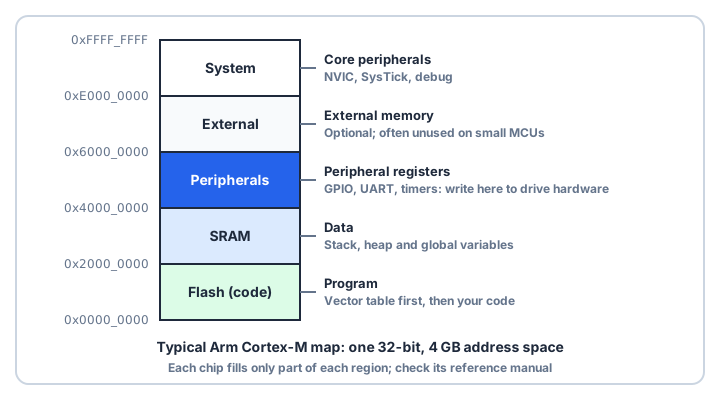
One address space
A Cortex-M uses 32-bit addresses, which gives a 4 GB space. Arm fixes what each region is for, so the layout is the same from one vendor to the next. A real chip fills only a sliver of it. An STM32F103C8, for example, has 64 KB of Flash at 0x0800_0000 and 20 KB of SRAM at 0x2000_0000. Reading an address where nothing is fitted triggers a fault.
Region by region
- Code (from
0x0000_0000): Flash, starting with the vector table. STM32 parts put Flash at0x0800_0000and mirror it at address 0 when they boot from Flash. - SRAM (from
0x2000_0000): the stack, the heap and global variables. - Peripherals (from
0x4000_0000): each peripheral owns a block of registers. Writing to these addresses changes the hardware. - External (from
0x6000_0000): for external memory controllers, usually unused on small parts. - System (from
0xE000_0000): the NVIC, SysTick and debug blocks, at the same address on every Cortex-M.
Where you meet it
The linker script tells the toolchain where Flash and RAM are, so it can place code and data:
MEMORY
{
  FLASH (rx)  : ORIGIN = 0x08000000, LENGTH = 64K
  RAM   (rwx) : ORIGIN = 0x20000000, LENGTH = 20K
}
And because peripherals are just addresses, this line drives pin PA5 high on an STM32F103, where the GPIOA output register sits at 0x4001_080C:
*(volatile uint32_t *)0x4001080C |= (1u << 5);The volatile keyword tells the compiler that every access matters, so it never caches or skips one. Vendor headers wrap these addresses in readable names like GPIOA->ODR.