 Microcontrollers & architecture
 3 min read
Harvard vs von Neumann
A von Neumann CPU fetches instructions and data over one shared bus, so each memory cycle is either a fetch or a data access. A Harvard CPU gives code and data separate buses, so it can fetch the next instruction while it reads or writes data.
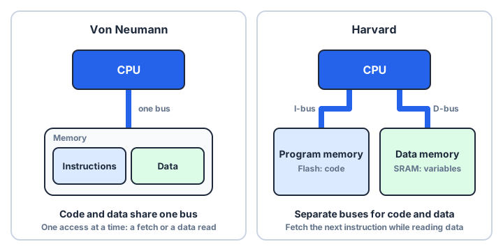
One road or two
The von Neumann design keeps the program and its data in the same memory and reaches both over one bus. It is simple and flexible: code can be loaded into RAM and run like any other data. The catch is the von Neumann bottleneck. When an instruction needs data, the next instruction fetch has to wait for the bus.
The Harvard design, named after the Harvard Mark I that read its instructions from punched tape, separates the two. With an instruction bus and a data bus working in parallel, a pipelined core can keep fetching while it works on data.
What real chips do
| Von Neumann | Harvard | |
|---|---|---|
| Buses | One, shared | Separate for code and data |
| Memory access | Fetch and data take turns | Fetch and data can overlap |
| Address spaces | One | Separate (pure Harvard) |
| Examples | Arm Cortex-M0 and M0+ | AVR, PIC, 8051 |
Most modern parts are a modified Harvard mix. An Arm Cortex-M3 or M4 has separate I-Code and D-Code buses for speed, but both reach the same 4 GB address space, so one pointer type can read anything. Desktop CPUs do the same thing inside the core with split instruction and data caches.
Why it shows up in your code
On a pure Harvard AVR, Flash and SRAM have separate address spaces. A const table is still copied into scarce SRAM at startup unless you mark it PROGMEM and read it with a special function:
const uint8_t table[] PROGMEM = { 1, 2, 4, 8 };
uint8_t v = pgm_read_byte(&table[2]);   // reads Flash via the LPM instruction
On a Cortex-M, the same const table simply stays in Flash and you read it with an ordinary pointer.